
Key takeaways:
- Novel electronic materials patent activity is shifting from materials discovery toward device integration, manufacturing, and semiconductor architecture innovation.
- Electromechanical materials dominate the patent landscape, accounting for 68% of patents, but their maturity leaves less room for broad, defensible new IP.
- Neuromorphic materials are emerging as a key growth area as AI hardware demand drives innovation in memory-compute architectures, CMOS compatibility, and device integration.
- Spintronics remains the second-largest patent category, with innovation moving beyond MRAM toward manufacturability, scalability, and circuit-level integration.
- Quantum and topological materials remain early-stage opportunities, with the greatest potential in materials optimization, scalable manufacturing, and CMOS-compatible device development.
Lux Take: Competitive advantage in novel electronic materials is shifting from materials discovery to device integration, manufacturing, and defensible IP
The competitive advantage in novel electronic materials is shifting from materials discovery to integrating new materials and chip architectures into devices and memory stacks. Semiconductor manufacturers and technology enterprises should prioritize licensing, joint venture agreements, or targeted IP in materials characterization and interfaces in neuromorphic, spintronic, and topological device architectures, while treating electromechanical materials as a mature incumbent-controlled category where new entrants will struggle to defend broad IP.
What patent activity reveals about the future of electronic materials
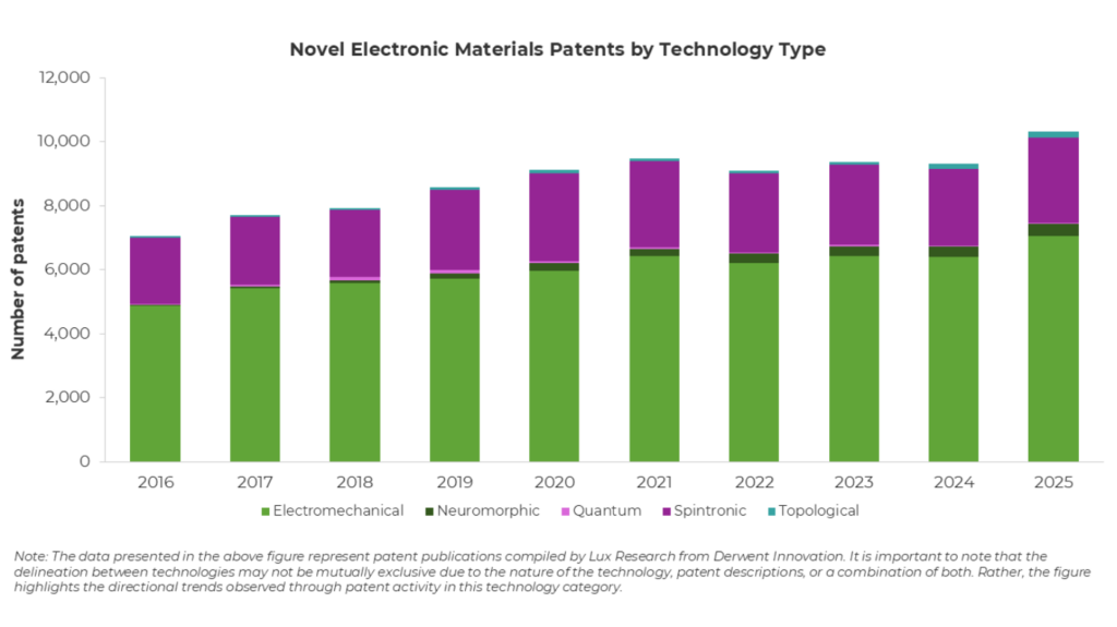
Patent activity in novel electronic materials has grown 4% annually since 2016, driven by bottlenecks in the power consumption, read/write performance, and sensitivity of conventional semiconductor devices. Demand for computing, industrial and consumer sensing, and efficient AI hardware continues to accelerate innovation across these materials. Although all five material categories target these bottlenecks, patent activity remains unevenly distributed. Electromechanical materials account for 68% of patents, reflecting their technological maturity and emphasis on device optimization. Neuromorphic and spintronic technologies maintain strong patent portfolios as foundational materials discoveries have progressed into device-level innovations, including neuromorphic cells and spintronic random access memory (RAM) stacks. In contrast, quantum materials have a small patent base that is more evenly split between materials innovation and device architectures. Topological materials show fluctuating patent activity because of their diverse applications and the technical challenges that limit commercialization and scale. Both quantum and topological materials remain early stage fields, with few startups gaining traction despite strong investment interest and substantial opportunities for materials-related IP. Overall, the patent landscape reflects technologies at different stages of maturity and is likely to shift toward less mature categories as they address the limitations of conventional electronic materials.
In this brief, we analyze novel electronic materials patents across electromechanical, neuromorphic, quantum, spintronic, and topological categories.
Patent trends shaping novel electronic materials
In this section, we analyze the patent trends for each of the categories individually and discuss how these trends may impact future innovation opportunities in this space.
Electromechanical materials dominate a mature patent landscape
Electromechanical patents form the mature core of the landscape, with five of the top six contributors being enterprises in the APAC region. The category accounts for 68% of all patents, with annual patent publications increasing 45% between 2016 and 2025. Solid-state devices, including piezoelectric materials and devices and microelectromechanical systems (MEMS), represent 45% of patents published over the past decade. APAC holds approximately 89% of electromechanical patents, reflecting strong commercial and academic investment. The leading filers are Murata, Epson, and Fujifilm, which focus on piezoelectric materials and integration, actuators and MEMS sensors, and thin-film materials, respectively.
Patent activity focuses on lead-free materials, temperature-resistant compositions, and materials that operate without a current bias, highlighting efforts to improve material composition, fault tolerance, and power efficiency. Sustained patenting in piezoelectric stacks, MEMS devices, and sensing technologies reflects mature technical capabilities for precision sensors, audio devices, and robotics. For example, TDK’s 2026 patent application on a lead-free piezoelectric material that operates without a current bias reduces power consumption. Similarly, Murata’s 2024 patent on a piezoelectric film manufacturing method and device demonstrates a shift from materials composition toward manufacturing and device integration. Given the category’s maturity and dense IP landscape, companies are more likely to create value through targeted licensing agreements and joint ventures than by developing competing technologies independently.
Neuromorphic materials show strong growth as AI hardware advances
Neuromorphic materials is the strongest growth signal in the smaller categories, but the low base still makes commercial readiness uncertain. Neuromorphic materials account for roughly 2.5% of all patents. APAC produces approximately 67% of neuromorphic patent publications, while IBM, headquartered in the U.S., leads all filers with 137 patents. The top three filers are IBM, Huazhong University of Science and Technology, and Nanjing University of Posts and Telecommunications.
Over the past decade, patent activity has shifted from proof-of-concept materials to device-level applications. For example, Samsung’s 2016 patent on a nonvolatile memory transistor preceded innovations in multi-bit, system-on-a-chip (SoC)-compatible neuromorphic cells and memory-compute architectures. Material composition remains a major focus, accounting for 40%–45% of patents annually, reflecting continued efforts to optimize performance through intrinsic materials properties. Leading organizations increasingly emphasize device development and integration, while key technical gaps remain in compatibility with complementary metal-oxide-semiconductor (CMOS) technology, power efficiency, and system sensitivity. Given these challenges, the strongest commercialization strategy is to partner with AI hardware and neuromorphic startups, sharing development risk while focusing on materials integration and device architecture.
Quantum materials offer early-stage opportunities for differentiated IP
Quantum materials remain an early stage patent landscape, with limited commercial activity and continued emphasis on fundamental materials research. The category accounts for roughly 0.7% of all patents and peaked at 115 annual publications in 2018. APAC and the Americas account for 57% and 26% of patent activity, respectively. Approximately 62% of patents focus on material composition and properties, underscoring the continued importance of materials optimization.
Arm, Cerfe Labs, and Samsung lead patent filings, focusing on quantum systems, sensing, and materials, respectively. Between 2016 and 2018, patent activity centered on materials engineering, correlated electron switches, and 2D semiconductor contacts, exemplified by Arm’s 2017 patent on correlated electron switches. Since 2018, innovation has shifted toward CMOS-compatible materials, Josephson junction devices, and scalable manufacturing. Cerfe Labs’ 2022 patent on a manufacturing method for correlated electron materials illustrates this transition from fundamental materials research to fabrication and device integration. White space in this category lies in materials optimization and fault-tolerant device development. Although academic institutions continue to dominate the field, a small number of well-funded startups have begun commercializing quantum materials, creating opportunities to build intellectual property around novel materials and integrated devices. Given the category’s early stage, the strongest commercialization strategies are to license enabling architectures or manufacturing methods and acquire startups with differentiated materials IP.
Spintronics shifts from MRAM innovation to scalable semiconductor integration
Spintronics is the second-largest patent category and is transitioning from foundational magnetoresistive RAM (MRAM) technologies to manufacturability, variability control, and circuit-level integration. The category accounts for roughly 28% of all patents, with annual activity peaking at 2,748 publications in 2020. APAC dominates patent filings, led by companies such as Taiwan Semiconductor Manufacturing Company (TSMC), Samsung, and TDK, which focus on embedded MRAM, memory devices, and magnetic multilayers, respectively.
Before 2020, patent activity centered on fundamental device structures, including magnetic tunnel junctions (MTJs), synthetic antiferromagnets, and spin-transfer torque MRAM. TSMC’s 2016 patent on synthetic antiferromagnetic reference layers for MTJs exemplifies this focus on core MRAM architectures. Since 2020, innovation has shifted toward spin-orbit torque MRAM (SOT-MRAM), with increasing emphasis on CMOS integration, manufacturing optimization, and device scalability. IBM’s 2023 patent on SOT-MRAM memory stacks reflects this transition. Key opportunities remain in novel spintronic materials and improved CMOS compatibility. Given the category’s technical maturity and dense IP landscape, the strongest commercialization strategies are to license foundational MTJ and memory-stack technologies while partnering with startups to develop and validate novel spintronic materials.
Topological materials offer long-term potential but face commercialization barriers
Topological materials remain an early stage patent landscape with broad application potential but limited commercial maturity. The category accounts for roughly 1% of patents published over the past decade, with APAC representing 66% of all filings. Patent activity spans diverse applications rather than converging on a dominant technology, reflecting continued exploration of the material platform.
Enterprises have adopted two distinct patenting strategies: specializing in a single application area or diversifying across multiple use-cases. IBM exemplifies the first approach, evolving from thin-film fabrication techniques to device-level integration, including its 2024 patent incorporating a topological conductor into a SOT-MRAM device. BOE represents the second strategy, with a 2016 patent applying topological materials in solar cells and a 2020 patent on a transparent organic LED panel using a topological insulator. Startup participation remains limited, with most patents originating from established companies or university-industry collaborations, indicating that the field remains too technically complex for widespread startup commercialization. The largest opportunities lie in scalable topological devices, crystal growth, and CMOS-compatible integration. Foundries and established technology companies are best positioned to commercialize these materials through co-development partnerships that integrate topological materials into SoC platforms while building IP around scalable manufacturing.
The future of novel electronic materials and semiconductor innovation
Over the next decade, electromechanical materials will remain the largest patent category, but innovation will shift toward incremental optimization rather than foundational materials discovery. As the category matures, patent activity will increasingly move to spintronic, neuromorphic, and topological materials, where challenges in device integration and manufacturability leave greater room for defensible IP. Neuromorphic technologies are likely to gain momentum as AI hardware demand accelerates innovation in CMOS compatibility, memory-compute architectures, and device integration. Spintronics will continue advancing beyond MRAM toward scalable manufacturing and circuit-level integration. Quantum and topological materials will remain early stage fields, with commercialization limited by fabrication complexity and device reliability. Across all categories, integrating novel materials into CMOS manufacturing will remain the primary technical challenge. Consequently, partnerships will increasingly focus on foundry access, manufacturing expertise, and IP, with startups supplying novel materials and enterprises providing fabrication and commercialization capabilities.
Frequently Asked Questions
Which novel electronic materials offer the strongest innovation opportunities?
Neuromorphic, spintronic, and topological materials offer significant opportunities as innovation shifts toward device integration, manufacturability, CMOS compatibility, and new memory and computing architectures. Quantum materials also offer potential for differentiated materials and device IP but remain at an earlier stage of commercialization.
How are patent trends changing in novel electronic materials?
Patent activity is increasingly moving from fundamental materials discovery toward manufacturing, device architectures, memory stacks, and semiconductor integration. Mature categories such as electromechanical materials are becoming more focused on incremental optimization, while neuromorphic, spintronic, quantum, and topological materials leave more room for defensible intellectual property.
Explore the next era of industrial innovation
Novel electronic materials are only one part of the technology landscape reshaping industrial innovation. Explore Lux Research’s insights into the technologies, market shifts, and strategic priorities that will define the next era of industrials and help companies identify where to invest, partner, and innovate next.
Explore the next era of industrials innovation